Final Project
Wr227
Gerald Nelson
New CMP Process
Only through continual improvement can a company hope to reach its potential, improve its customer base, and ensure future profits. It is important that engineers, management and technicians involved in problem solving cycles and upgrades are familiar with the technological advances and research occurring in semiconductor manufacturing. New process and tools are being made available that could significantly cut costs and accelerate production through loss of downtime, reworks and machine failure.
Due to increased competition it is necessary to streamline production and upgrade tools in CMP (Copper Mechanical Polish). Because of the nature of the process the CMP step is one of the most expensive in semiconductor manufacture. It requires constant flow of expensive slurries, plus high preventative maintenance costs. Chips produced with 8 metal layers will go through the CMP process at least 9 times.
“Applied
Materials Inc. has announced what it says is a major breakthrough in
planarization technology. The company's 300mm Applied Reflex ion LK Encamp
system offers electro-chemical mechanical planarization capability on Applied's
Reflexion LK platform. The system is the industry's first CMP tool to provide a
high-performance, cost-effective and extendible system for copper/low k
manufacturing at 65nm and beyond.”(
Figure 1
Applied Materials
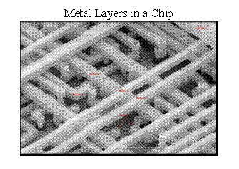
Copper CMP enables photolithography to achieve high resolution for small features on the surface of the wafer. With a rough wafer surface the depth of focus requirement of optical tools cannot be met. The planarization step is needed in order to lay down more metal layers on the chip (see figure 2).
Figure 2
LSI inc.
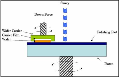
CMP planarizes the surface using chemical oxidizers abrasive slurries, and special pads. Uniformity of removal is mainly determined by the down force pressure distribution (see figure 3).
Figure 3
Brewer science, 2004
ECMP planarizes wafers with minimal down force. The copper is removed electrically from the wafers. It is an electrochemical method of removing metal ions from the surface by giving the wafer a positive charge. Only metal is removed in this process not the dielectric(insulator) silicone dioxide Using an electrolytic solution and an applied voltage the ECMP system passes copper into solution and two electrons are released as Cu àCu 2+ (complex) + 2 e- ( Dr. Liang Chen, Applied Materials p. 138)
The one drawback to this procedure is that the wafer must be planar at the beginning of the process. This would require a bulk copper removal CMP step. However, there are many benefits to ECMP.
- minimal dishing and erosion
- Less chatter and micro scratch.
- Reduced delamination on wafer.
- Reduced machine wear
- Reduced preventative maintenance
- Inexpensive slurries
- Simplified recipes
- Fewer production problems.
- Increased speed of copper removal.
- Superior quality of product
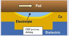
The down force used in CMP causes dishing and erosion (Figure 4). The dishing and erosion in wafers hinders photolithography. Dishing over large surface areas with copper occurs because there is less resistance in the copper than in the silicon dioxide. Causes of dishing are the variation in hardness of materials. Oxide is harder (less malleable) than copper or aluminum, therefore, when CMP breaks through the overlying oxide exposes the metal, and dishing occurs.
Figure 4
Dishing occurs because the copper is softer than
the surrounding material
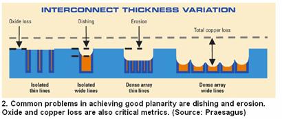
Peter Singer, Editor-in-Chief -- Semiconductor International,
“One way to reduce pattern dependencies in CMP
is to simply change the pattern layout by adding dummy fill structures. This
may not sound like an elegant engineering solution, but it dramatically reduces
CMP process variation and has further potential: "A number of companies
have not yet optimized their dummy fill algorithms to reduce variation. Even
the more sophisticated ones we see today in production tend to use
density-based dummy fill methodologies," said Taber Smith, president of
Praesagus (San Jose), a company that supplies characterization wafers and
design for manufacturing software that helps designers understand how process
variations such as pattern dependencies in CMP and plating can impact their
design.”( Peter Singer, Editor-in-Chief -- Semiconductor International,
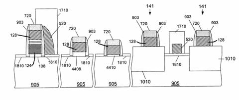
To counter dishing and erosion, dummy structures have been incorporated into chip design.(Figure 5) The dummy structure supplies metal interconnects where none would normally exist. This causes a more “even” removal of material.
Figure 5
Added dummy metal
interconnects to control the planarization process
![]()
(Hsing Ti Tuan, Cupertino, Calif. (US); and Chung Wai Leung,
Milpitas, Calif. (US)
Assigned to Mosel Vitelic, Inc., Hsin-Chu (
Filed on
The necessity of dummy structures to control material removal would be unnecessary using Electrical Chemical Mechanical Polish (Figure 6). “Ecmp provides sharply reduced dishing compared with conventional CMP on a wide 220-um line (without dummy features) and tight dishing range for die measured at the center, middle and edge of the wafer.” (Dr. Liang Chen, Applied Materials p. 138)
Figure 6
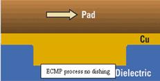
Semiconductor International,
Figure 4
“Chatter and micro scratch are also results of down force.(Figure 7) A common problem associated with the chemical-mechanical planarization (CMP) processes used in damascene sequences is the generation of microscratches. Microscratches form small trenches in the oxide, which are filled with tungsten during CMP processing. These metal-filled trenches, in turn, can short the intended patterned circuitry.”( Heinrich Ollendorf, Stacey Cabral, and Robert Fuller, 1992-2003)
Figure 7
Shorted out circuitry must be
corrected by expensive rework or the particular die with the microscratch will
have to be discarded. Microscratches reduce product yield and/or productivity.
MICRO Magazine © 1997-2003
Machine wear:
Because ECMP does not employ down force in the planarization of wafers there will be less wear on the machine parts of the tool. Motor bearings, platen bearings and transmissions, will have extended life. This will reduce tool downtime, production loss and repair costs.
Preventative Maintenance:
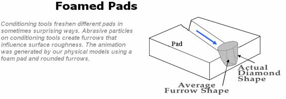
CMP uses polishing pads and pad conditioners in the planar process. The pads are made of foam material and are refreshed by the conditioners (Figure 6). The polish head holds the wafer in place and is also a consumable. The heads have a limited life and are expensive to replace.
Pads, conditioners, and heads are replaced periodically for continued quality of the process. The replacement requires downtime for the tool. At maintenance completion, a tool is qualified before product can be run. Qualifying is a time consuming and costly procedure. ECMP has a longer pad, head and conditioner life. The pads are less aggressive and have no down force applied to them. There is less maintenance with ECMP and therefore less downtime and increased production.
Figure 8
2003 Intelligent Planar
Slurries:
“ Slurry chemistry is the primary factor affecting removal selectivity in the CMP process. Removal selectivity is the rate at which slurry will remove one material compared to another, therefore slurries are configured for particular applications”.(Hong Xiao, p.529) Slurry is a high cost consumable in CMP process. It must also be treated before being returned to the environment. The slurry for ECMP is an electrolyte. Applied materials reports cost differences of over 40 %( See Figure 9) (Dr. Liang Chen, Applied Materials p. 138)
Figure 9
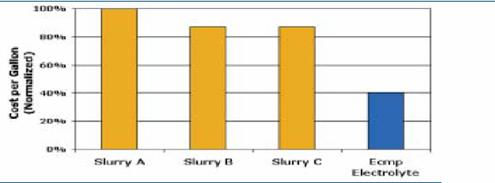
(Dr. Liang Chen, Applied Materials)
Production problems.
With CMP, process aborts are common. Aborts cause loss in production time due to diagnosis, repair, rework, and requalification. Most abort issues on CMP are related to down force and uneven copper removal.
ECMP has fewer aborts because there are fewer down force issues. Pads and heads are under less force because of less down pressure.
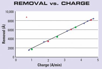
Increased speed of copper removal:
The polish rate is proportional to the current density; the higher the current density, the higher the polish rate. It will only remove the conductive material such as copper. No dielectric material can be removed during the electro polishing process,
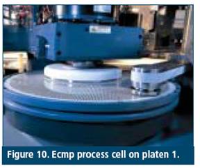
The removal rate is
controlled by the charge.(Figure 10) .The efficiency of the process cell
creates close to 100% ionization, which means all the copper is accounted for.
Since all of the copper is accounted for there is a very predictable and repeatable
process. (Peter Singer, Editor-in-Chief -- Semiconductor International,
Figure 10
( Dr. Liang Chen, Applied Materials)
This process warrants closer examination by engineering. ECMP offers reduction in consumables and maintenance with greater throughput. Lower production costs and superior results using ECMP would make our product more competitive both by reducing final costs and producing a superior product.
References:
Dr. Liang Chen, Applied Materials, Semiconductor Fabtech, 24th Edition
Hong Xiao, 2001. Introduction to semiconductor manufacturing technology: Prentice-Hall
Peter Singer, Editor-in-Chief -- Semiconductor International,
Heinrich Ollendorf, Stacey Cabral, and Robert Fuller,
Infineon Technologies MICRO Magazine © 1997-2003 Canon Communications LLC
All rights reserved.
Copyright 2003 Intelligent Planar ©. All Rights Reserved
Applied Boasts Planarization Breakthrough Online staff -- Electronic News,
© 2004 Reed Business Information, a division of Reed Elsevier Inc.
Author: Gerald Nelson